Great history of the small Bosch MEMS sensors
Ideal companions


They are extremely small and capable of registering every little thing. Yet they rarely make their presence known, are completely silent, and prefer to remain in the background.
For some, they may sound like the ideal companion. And as a matter of fact, they are. Life these days would be pretty inconceivable — not to mention slow and complicated — without electronic microsensors, or MEMS sensors. Capable of reacting to even the slightest changes, they can be found hidden away in cell phones, hard drives, cameras, airbags, ESP systems, pacemakers, and much more.
Micro-Electro-Mechanical-Systems
The abbreviation MEMS stands for “microelectromechanical systems,” which says a lot about these tiny helpers. MEMS are sensors that are capable of processing mechanical, magnetic, or even chemical changes in electrical input. In that sense, they are much like human beings, who are constantly receiving and processing external and internal stimuli. But while people are born with a sophisticated stimulus processing system, MEMS had to be engineered and developed first before they could enter mass production.

Combs smaller than strands of hair
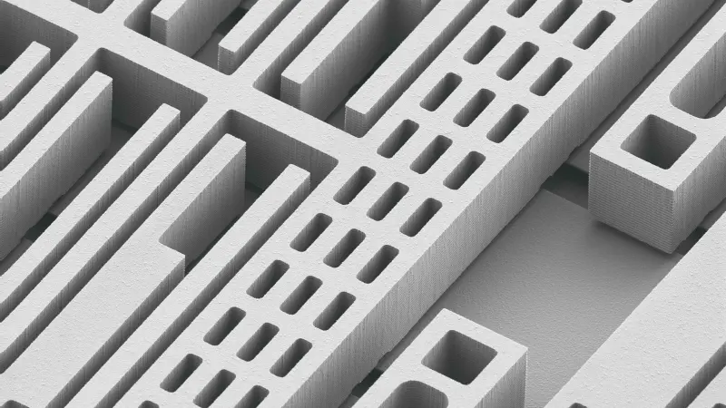
When laypeople look at devices such as acceleration sensors or yaw-rate sensors, all they can see is micrometer upon micrometer of tiny, odd-looking structures that form intricate patterns. Sometimes those patterns have a flat, single-level structure. However, many MEMS feature three-dimensional, deeply etched structures consisting of fixed and movable actuators known as “combs,” which can move in a variety of different directions depending on their purpose. In an airbag, for instance, the sudden and severe deceleration generated during an accident triggers a shift in the movable combs. The sensor reports this change in the status quo to the airbag control unit, instructing it to inflate the airbag immediately. Another, less dramatic example is the way a tablet’s screen rotates instantly when you move it.
Although MEMS work differently depending on their specific function, they are all based on a common principle: using movable, chemical, or magnetically sensitive components, changes in the status of the MEMS element — down to the nearest micrometer — are recorded and processed as electrical signals, triggering predefined actions.

Etching out a breakthrough
If you think manufacturing such highly sophisticated, minuscule components is tricky business, then you are right. Developing three-dimensional MEMS was a tremendous challenge that called for bright minds and a bold vision. In the early 1990s, a team of researchers at Bosch ultimately succeeded in doing the impossible, at least according to conventional wisdom: mastering the art of embedding moving structures in silicon to act as sensors. They also found a way to ensure the fast and high-precision mass production of products featuring these sophisticated structures. The result was a groundbreaking process for the industrial production of three-dimensional MEMS — one that Bosch would implement in Reutlingen in 1995.
Producing these tiny sensors involves a four-stage process with several hundred individual steps that takes many weeks. The silicon is processed in the form of ultra-thin discs known as wafers. By etching and depositing material, a variety of high-precision structures with depths of up to several hundred micrometers can be embedded on the silicon, creating chips with structures thinner than a human hair. Production has to take place in ultra-clean clean rooms, as even the tiniest particle of dust has the potential to interfere with the proper functioning of these sensitive systems.
The choice of silicon as a material was no accident, since it has mechanical properties that can be easily exploited. Bosch was already familiar with silicon from the production of integrated circuits in Reutlingen. For example, silicon’s elastic fibrous structure does not wear out – unlike with steel. Along with these advantages, large quantities of silicon can be found in grains of sand, making it inexpensive to produce.
The number of chips that can be mounted on a wafer per manufacturing cycle depends on the size of the wafer. Bosch introduced 6-inch wafers (150 millimeters) in 1995. Depending on the size of the components, a 6-inch wafer can hold up to 6,000 chips. In 2010, Bosch added 8-inch wafers (200 millimeters) to its portfolio. The company built a new factory in Reutlingen to make these larger wafers, which can now accommodate up to 50,000 microchips. Thanks to the method also known as the “Bosch process,” these wafers can be economically mass produced. Small sizes are possible, with consistent quality assured. What is more, they are ultra-precise, reliable and durable, all while consuming little energy despite the wide range of uses.
The hidden key to the future of technology
The first MEMS to start leaving the Reutlingen plant in 1995 were pressure sensors for the automotive industry. They were joined by sensors for airbag activation in 1996 and for the electronic stability program (ESP®) in 1998. Today, every modern automobile contains an average of five Bosch MEMS sensors.
Great strides have also been made in the development of these mini-sensors for other applications. They are an essential part of everyday objects such as consumer goods, electrical appliances, fitness trackers, and many other devices. MEMS therefore ultimately play a crucial role in the connectivity of devices. The internet of things would be unthinkable without them.


Today Bosch has already manufactured more than 15 Billion sensors, making it the global market leader for this key technology of the future. And because Bosch covers the entire value chain — from the development of the MEMS processes, sensor design, and evaluation circuits, all the way through to their packaging, test procedures, production, and sale — the company has deep knowledge of these miniature marvels of technology and the complex way their functions are interconnected, no matter what role they may play in the background.
Author: Vera Dendler

