Bosch opens chip factory of the future in Dresden
#BoschSiliconDay: First wafers pass through fully automated fabrication process

2021-06-04
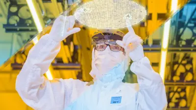
It is a milestone on the path to the chip factory of the future: at the new Bosch semiconductor fab in Dresden, silicon wafers are passing through the fully automated fabrication process for the first time.
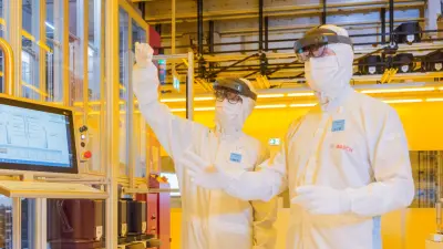
Manufacturing of automotive microchips will be a primary focus when the fully digital and highly connected semiconductor plant is up and running. “Chips for tomorrow’s mobility solutions and greater safety on our roads will soon be produced in Dresden. We plan to open our chip factory of the future before the year is out,” says Harald Kroeger, member of the board of management of Robert Bosch GmbH. The company already operates a semiconductor fab in Reutlingen near Stuttgart. The new wafer fab in Dresden is Bosch’s response to the surging number of areas of application for semiconductors. Bosch is investing around one billion euros in the high-tech manufacturing facility, which will be one of the most advanced wafer fabs in the world.
Follow blogger Nicole Scott on a virtual video tour of the fully connected and intelligent Waferfab in Dresden.
Loading the video requires your consent. If you agree by clicking on the Play icon, the video will load and data will be transmitted to Google as well as information will be accessed and stored by Google on your device. Google may be able to link these data or information with existing data.
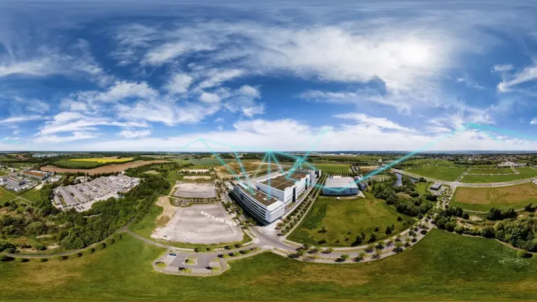
360° Waferfab
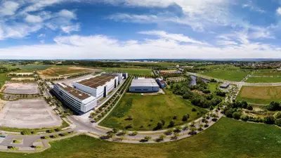
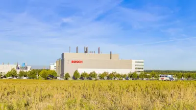
The new Bosch plant stands on a plot the size of 14 football pitches. Production and office space is being built on a total of 72,000 square metres. Take a look inside and explore the waferfab with interactive sphere photos, almost as if you were on site.
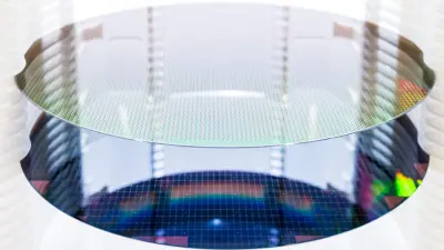
300-millimeter fab
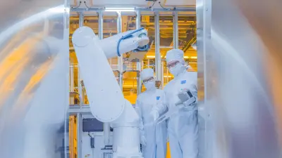
The technology in focus at Bosch’s new Dresden facility is 300-millimeter fabrication, in which a single wafer can accommodate 31,000 individual chips. Compared with conventional 150- and 200-millimeter wafers, this technology offers the company greater economies of scale and boosts its competitiveness in semiconductor production. Moreover, fully automated production and real-time data exchange between the machines will make chip manufacturing in Dresden exceptionally efficient. “Our new wafer fab sets standards in automation, digitalization, and connectivity,” Kroeger says.
From wafer to chip
Semiconductors are finding their way into more and more applications, including in the internet of things and for mobility of the future. The semiconductor fabrication process begins with round discs of silicon known as wafers. At the Bosch fab in Dresden, these wafers have a diameter of 300 millimeters and, at just 60 micrometers thick, will be thinner than a human hair. To produce the coveted semiconductor chips, the untreated – or “bare” – wafers are then processed for several weeks. As the application-specific integrated circuits (ASICs) in vehicles, for instance, these semiconductors act as the vehicle’s brains. They process the information from sensors and trigger further actions, such as sending a lightning-fast message to the airbag to tell it to deploy. Although the silicon chips measure just a few square millimeters, they contain complex circuits, sometimes featuring several millions of individual electronic functions.
Podcast: How to build one of the cleanest places on Earth — in dialogue with the fab’s project manager, Otto Graf
![From KNOW-HOW to WOW - The Bosch Global Podcast [Episode 11 Part I]](https://assets.bosch.com/media/global/stories/bosch_chip_factory_dresden/youtube-preview-zpsxxnuvuow_res_768x432.webp)
Loading the video requires your consent. If you agree by clicking on the Play icon, the video will load and data will be transmitted to Google as well as information will be accessed and stored by Google on your device. Google may be able to link these data or information with existing data.
First AIoT factory
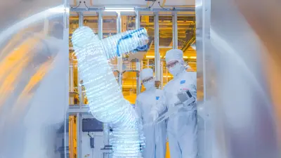
The Dresden wafer fab is Bosch’s first AIoT factory. AIoT stands for the combination of artificial intelligence (AI) and the internet of things (IoT). With this, Bosch is creating a sound basis for data-driven, continuous improvement in production, and setting new standards for Industry 4.0. Artificial intelligence methods can be used to evaluate the data generated in the wafer fab. For example, an AI algorithm can detect even the tiniest anomalies in products. These anomalies are visible on the wafer surface in the form of specific error patterns known as signatures. Their causes are immediately analyzed and deviations from the process corrected without delay, even before they can affect the reliability of the product. This is the key to further improving the manufacturing processes and semiconductor quality, as well as to achieving a high level of process stability. In turn, it means that semiconductor products can go into full-scale production quickly. Furthermore, AI algorithms can precisely predict whether and when a piece of manufacturing machinery or a robot needs maintenance or adjustment. In other words, such work is not done according to a rigid schedule, but precisely when it is needed — and well in advance of any problems cropping up. AI is also used in production scheduling, saving time and costs as it guides the wafers through several hundred processing steps at roughly 100 machines in the plant.
Plant with “digital twin”
Manufacturing of automotive microchips will be a primary focus when the fully digital and highly connected semiconductor plant is up and running. “Chips for tomorrow’s mobility solutions and greater safety on our roads will soon be produced in Dresden. We plan to open our chip factory of the future before the year is out,” says Harald Kroeger, member of the board of management of Robert Bosch GmbH. The company already operates a semiconductor fab in Reutlingen near Stuttgart. The new wafer fab in Dresden is Bosch’s response to the surging number of areas of application for semiconductors. Bosch is investing around one billion euros in the high-tech manufacturing facility, which will be one of the most advanced wafer fabs in the world.
Looking through data glasses
In its Dresden plant, Bosch is making use of augmented reality (AR). Thanks to smart AR glasses and tablets, users will be able to see digital content superimposed on the real environment. For example, an AR app developed by Bosch allows energy data from the wafer fab to be displayed in a virtual model of the building. This makes it possible to optimize the carbon footprint of the manufacturing machinery. Data glasses also help with construction planning, and in the future will be an important aid for remote maintenance of the machinery and systems by experts who may be thousands of miles away.
5G-ready
To make the transmission of data between machines and computers even more flexible, the new 5G mobile communications standard will soon be introduced at the semiconductor plant. The plant was 5G-ready right from the start: all the requirements for 5G infrastructure were taken into consideration during the construction phase.
Carbon neutral from the start
Environmental protection and sustainability were priorities at the new location from day one. This is why the Dresden wafer fab will be carbon neutral from the outset. To achieve this, Bosch can build on experience gained at the sister plant in Reutlingen. For example, its primary energy supply is exclusively in the form of green electricity and carbon-neutral natural gas. Furthermore, sophisticated energy management ensures the best possible power consumption in its manufacturing operations.