Humans and machines team up in the factory of the future

Machines that think for themselves, maintenance from a distance of 9,000 kilometers, glasses with built-in cameras — one of the world’s most advanced wafer fabs in Dresden features all this and more. Tests have been underway since early 2021 at this facility where Bosch intends to manufacture the key technology for tomorrow’s mobility. Data scientist Sarah Fischbach tells the story of how humans and machines work as a team to make these semiconductors.
Industry 4.0 showroom: the smart factory of the future in Dresden
Loading the video requires your consent. If you agree by clicking on the Play icon, the video will load and data will be transmitted to Google as well as information will be accessed and stored by Google on your device. Google may be able to link these data or information with existing data.

Unseen but ubiquitous, semiconductors in the form of microchips figure prominently in smartphones, televisions, dishwashers, and just about every other technical device. This includes cars: these days, Bosch chips can be found in almost every car in the world, in airbags, braking systems, parking assistants, and the like. As automated and electric vehicles make inroads, the automotive sector is going to need many more and far more powerful microchips. Bosch is responding to this demand in several ways, one being this new fab in Dresden. With a price tag of around one billion euros, this futuristic factory is the largest single investment in the company’s 130-plus-year history. Highly automated, this plant opens the door to a new dimension in manufacturing where total connectivity provides the means to make planning, production, and delivery even more efficient. And that takes state-of-the-art technologies and well-trained experts. Sarah Fischbach, a data scientist at Dresden, is one such specialist.
Six weeks to a microchip
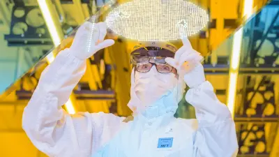
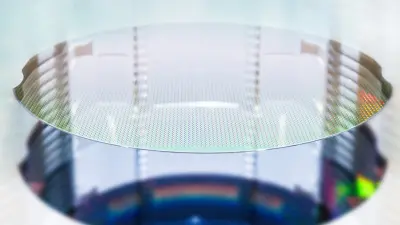
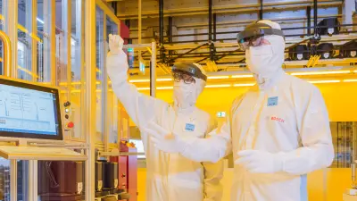
The job of Sarah and her team is to continuously optimize wafer production. Just one millimeter thick, the 300-millimeter silicon discs on which microchips are built in a six-week production process at the Dresden fab are called wafers. Bosch has been using wafers with diameters of 150 and 200 millimeters for some time now at its Reutlingen fab. The Dresden fab can manufacture even more microchips in every production run with its 300-millimeter wafers. These chips are destined for Bosch products in the domain of automated driving and will enable connectivity in other products. Bosch is the only automotive supplier in Europe to manufacture semiconductors of its own. “It's fascinating to see what’s already possible with our microchips,” says Sarah.
380 km
of electrical cables connect every part of the fab
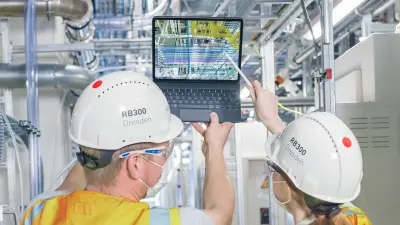
“What makes this fab so special is the interplay of two technologies,” says Sarah, talking about artificial intelligence and the internet of things, whose combination results in the acronym AIoT. The Dresden fab is Bosch’s first AIoT factory. All its systems, sensors, and products generate data, which is collected in a central repository. The data quantities are enormous: every second, the plant generates the equivalent of 500 pages of text. That would amount to more than 42 million sheets of paper a day — big data indeed. This is where artificial intelligence comes in, as self-optimizing algorithms learn to make predictions based on the data. In this way, operations can be analyzed in real time without disrupting sensitive manufacturing processes.
Semiconductor manufacturing processes are complex. It all starts in the sub-fab, an area below the actual wafer fab fitted with equipment to provide gases, air, and electricity to the chamber above. Kilometers of pipes, cables, and hoses run through the sub-fab. Every pipe, cable, and hose has a digital counterpart, as does each valve and every other component throughout the plant. The entire building is mapped to a 3D model in exacting detail. This model is enhanced with other information such as consumption data to create a digital twin — that is, a virtual rendering of the plant and all its processes. “This enables us to simulate optimizations and structural alterations in the virtual realm without having to disrupt processes in the real world,” says Sarah.
No air shower, no entry
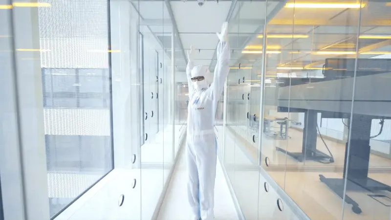
Before Sarah can enter the heart of the fab, the cleanroom, she has to first slip into a special white coverall. Then she has to step into an air shower that blasts away every last speck of dust. Only then is she allowed to pass through the airlock to the chamber where the semiconductors are conveyed in wafer boxes. This area requires cleanroom class 1 conditions. The usual number of airborne particles, some 100,000 per cubic foot, is unacceptable here. A cubic foot of fab air — or around 28 liters — may contain no more than one particle weighing just half a microgram. To put this into perspective, that equates to a single cherry pit floating in Lake Constance, which holds about the same as 360 million bathtubs.
It all comes down to the human factor
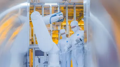
“This is where the intensive work gets done — mainly by the equipment,” says Sarah with a chuckle. Nearly everything in the cleanroom is automated. An autonomous conveyor system takes the wafers from one processing step to the next. Robot arms dip them in liquids; colossal microscopes scan them independently at the end of the line. An AI-powered algorithm that detects even the slightest imperfections inspects images, scanning for defects called signatures on the wafer. Sarah and her colleagues step in when it picks up on any defects. “We analyze the root cause and make the decision.” No matter how advanced the technology may be, ultimately the human factor still matters — even if machine learning methods assist in important ways. They not only detect process anomalies before they can affect a product’s reliability; they can also optimize the wafer production sequence to increase throughput.
“We trust the technology. But the critical decisions are always made by humans.”
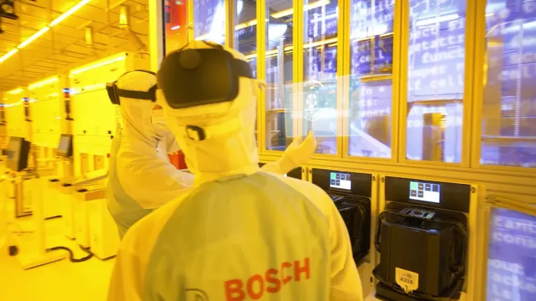
Data glasses facilitate maintenance
Even the most advanced machines require maintenance. However, these tasks can be optimized and executed just in time with predictive maintenance and AIoT. AI algorithms can pinpoint necessary repairs at an early stage based on the collected usage data. This work is not dictated by a set schedule but performed precisely when needed — in good time, before problems occur. A machine may even be maintained remotely using data glasses and augmented reality. For example, a specialist at an equipment manufacturer in Japan could perform maintenance work in Dresden without having to actually be there in person. The camera mounted on the data glasses transmits video images to Japan, allowing the expert there to guide the technician at Dresden through the maintenance task in real time.
The wafer fab will soon communicate via the new 5G mobile cell standard to accelerate these processes and data transfer between machines and computers. This is just one of several advances that feature prominently in the plans of the Dresden-based team of some 250 people. It also intends to use AI to develop and simulate entirely virtual prototypes before ramping them up for production. This way, Bosch will be able to set new quality standards, speed up the development process, and cut costs. What will it take to make that happen? State-of-the-art technologies and highly capable associates. Or as Sarah Fischbach puts it, “People and technology are one team in Dresden — and together, we’re stronger.”
Profile

Dr. Sarah Fischbach
Data scientist in product engineering at the Bosch wafer fab in Dresden
“This blend of wafer production, data analysis, and machine learning is the perfect combination for me.”
Sarah Fischbach studied physics and had already researched semiconductor technology when working on her doctorate at TU Berlin. The project to build the new Bosch plant in Dresden was her next challenge, and an exciting one at that. Determined to optimize product quality, this AI expert has been focusing on wafers and wafer manufacturing processes in the factory of the future since 2018.